
ITO coated glass is glass carrying a thin film of indium tin oxide, applied so the surface stays optically transparent while conducting electricity. Engineers specify it wherever a circuit needs to see through its own electrode, from touch panels to OLED displays and EMI shielding windows. The trade-off is consistent across every application: mechanical fragility, a thermal ceiling near 350°C, and exposure to the volatile cost of indium supply.
TL;DR:
- Sheet resistance should be specified alongside transmission percentage and film thickness because two films with the same resistance can differ significantly in transparency.
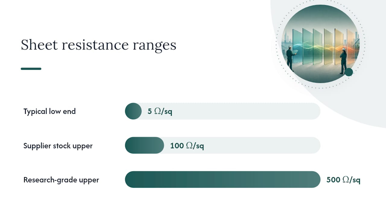
- The typical sheet resistance range for commercial ITO glass spans from about 3 to 100 Ω/sq, suitable for most touch panels and displays, with higher resistance grades used mainly for research.
- ITO coating quality depends heavily on manufacturing conditions, measurement map accuracy, and environmental aging tests, which are crucial for predictable performance.
- Alternatives like FTO, AZO, or nanowire networks may be preferable for high-temperature processing, flexibility, or indium supply issues, but each carries trade-offs in conductivity, transparency, or cost.
- Proper RFQ and sampling procedures, including detailed test reports and visual sample maps, are essential to avoid costly field failures and mismatched specifications.
Table of Contents
- What are the key properties of ITO coated glass?
- How is ITO coated glass made?
- What substrate and datasheet specs should you request?
- How is ITO patterned and customised?
- Where is ITO coated glass actually used?
- When should you choose an alternative to ITO?
- What tests should you demand from a supplier?
- How do you write an RFQ for custom ITO coated glass?
- How Precision Glasses approaches ITO coated glass supply
- Get custom ITO coated glass specified and quoted
- The gap between an ITO spec sheet and a working part
- Sources
What are the key properties of ITO coated glass?
Sheet resistance and optical transmission move in opposite directions, and every specification decision comes back to that tension. A thicker indium tin oxide film lowers sheet resistance but absorbs and scatters more light, so the engineer’s job is picking the point on that curve that suits the application rather than chasing the lowest resistance available.
Suppliers grade ITO glass across a wide sheet resistance band. Commercial products range from roughly 5 Ω/sq at the low end up to 500 Ω/sq for research-grade films, with transmission figures typically exceeding 80 to 90% at 550 nm depending on how thick the coating runs. Stocked catalogue glass tends to cluster around a narrower band. Standard suppliers commonly stock sheet resistances from 3 to 5 Ω/sq up through 100 Ω/sq, which covers most touch panel and display work without a custom run.
Pro Tip: Never specify sheet resistance alone. Always pair it with the film thickness and the transmission percentage at 550 nm, because two films with identical Rs can differ in transparency by several percentage points depending on their crystallinity and thickness.
Beyond resistance and transmission, four figures matter for design work including work function, which influences charge carrier injection or collection at OLED or photovoltaic junctions.
- Surface roughness: RMS roughness above a few nanometres starts to scatter light measurably and can affect adhesion of subsequent layers.
- Haze: acceptable haze thresholds tighten sharply for optical and display-grade parts compared with EMI shielding windows.
- Thermal ceiling: film resistivity begins to drift once processing or operating temperatures climb past roughly 350°C, a limit that shapes everything downstream, from lamination to soldering.
Film thickness ties all of this together. Thin films (sub 50 nm) transmit more light but carry higher resistance; thicker films (up to 300 nm) push resistance down at the cost of transmission and flexibility.
How is ITO coated glass made?
Magnetron sputtering, run in either DC or RF mode, is the dominant industrial deposition method for high-quality ITO films. The dominant industrial route uses a sputtering target composed of In2O3:SnO2 in a 90:10 weight ratio, with film thickness engineered according to sheet resistance requirements.
The process itself follows a fairly consistent sequence, though every supplier tunes the specifics:
- Substrate cleaning. Glass is degreased, ultrasonically cleaned, and often plasma-treated to strip contaminants that would otherwise create pinholes or adhesion failures in the film.
- Chamber evacuation and gas mixing. The chamber is pumped to a controlled base pressure, then backfilled with an argon and oxygen mixture, where the oxygen partial pressure has an outsized effect on carrier concentration and optical absorption.
- Sputtering. DC or RF power ionises the target material, depositing ITO onto the moving or stationary glass substrate at rates governed by power density and gas pressure.
- Post-deposition annealing. Heating the coated glass, typically in the low hundreds of degrees Celsius, improves crystallinity, which lowers resistivity and can improve transmission simultaneously.
Published lab protocols document cleaning sequences, base pressures, RF power settings, and annealing temperature ranges providing useful reference points for manufacturing specifications.
Glass isn’t the only substrate in play. Where flexibility or heat sensitivity rules out standard sputtering temperatures, low-temperature plasma-assisted deposition can produce sheet resistances below 10 Ω/sq on plastic substrates at process temperatures under 100°C, opening the door to flexible touch sensors. Electron-beam evaporation and pulsed laser deposition remain viable alternatives for smaller research runs, though neither scales as economically as sputtering for volume production.
What substrate and datasheet specs should you request?
Substrate choice is rarely arbitrary. Soda-lime glass covers most touch panel and general electronics work at the lowest cost. Borosilicate steps in where thermal shock resistance matters, typically in lighting or instrumentation housings. Fused silica earns its premium price in UV-transmitting optics and high-precision scientific instruments, and sapphire appears where scratch resistance outweighs everything else, as in certain sensor windows and rugged displays. Full technical glass options and their trade-offs are worth reviewing before locking in a substrate for a new design.
A complete datasheet request should specify, at minimum:
- Sheet resistance with a stated tolerance (commonly expressed as Rs ± a percentage)
- Transmission percentage at 550 nm, and ideally across the full visible band
- Film thickness in nanometres
- RMS surface roughness
- Haze percentage
- Work function, where the application involves charge injection
- Adhesion test results, referenced to a named standard
Handling notes matter as much as the numbers. ITO coated glass chips at the edges more readily than uncoated glass of the same thickness, so cutting and edge-finishing steps need to be specified up front rather than assumed. Confirm which face carries the coating on every shipped panel, since a reversed part is a common and costly assembly error, and request clear pack labelling that states coated-side orientation, batch number, and test date for traceability back to the production run.
How is ITO patterned and customised?
Three routes dominate ITO patterning, and each carries a different resolution ceiling and a different set of risks.
- Wet chemical etching uses acid-based etchants and is the lowest-cost route for coarse patterns, but etchant chemistry needs checking against any adjacent metal layers or adhesives on the same part.
- Laser ablation removes ITO with a focused beam, reaching fine features quickly without photoresist, though the heat-affected zone around each cut can degrade conductivity at the pattern edge if power isn’t controlled carefully.
- Photolithography delivers the finest features and supports multilayer stacks, making it the standard choice for high-resolution touch sensors and OLED backplanes, at a higher unit cost than the other two routes.
Design margins deserve attention before a pattern goes to production. Contact pads need enough area to keep contact resistance low and stable across thermal cycling, busbars should be sized against the current the application actually draws rather than a generic rule of thumb, and via placement needs a clear keep-out zone from pattern edges to avoid stress concentration during handling. A custom patterning and design review process at the pilot-run stage catches most of these issues before they reach volume production.
Where is ITO coated glass actually used?
Application requirements diverge sharply once you move past the basic material properties, and matching Rs and optical specs to the right application class avoids over-specifying (and overpaying for) a part.
- Touch panels generally target sheet resistance in the 100 to 300 Ω/sq range, balancing response time against transparency, with patterning resolution driven by the sensor’s touch grid density.
- Displays, particularly top-emission OLEDs, push toward lower resistance. High-brightness OLED designs commonly specify ITO with anti-reflection coatings and low sheet resistance to hit luminance targets while controlling RC delay across the panel.
- Photovoltaics trade sheet resistance against optical transmission at the cell’s active wavelengths, and the ITO layer’s interaction with the recombination layer beneath it affects overall cell efficiency, not just the coating’s own conductivity.
- EMI shielding and aerospace or medical observation windows favour very low sheet resistance. ITO films near 5 Ω/sq can deliver meaningful shielding across the 100 MHz to 10 GHz band while keeping visible transmission above 80%, a combination that matters for cockpit displays and imaging equipment alike.
- Biosensors and microfluidic devices typically call for thin ITO films that stay compatible with microscopy and downstream surface chemistry, prioritising optical clarity and biocompatible surface treatment over raw conductivity.
Display cover glass and touchscreen selection carry their own mechanical and optical constraints worth reviewing separately, particularly around how cover glass interacts with the underlying ITO layer in finished assemblies.
When should you choose an alternative to ITO?
ITO’s limitations cluster around three points: mechanical fragility under repeated flexing, a thermal ceiling that constrains processing, and exposure to a raw material whose price swings with global supply.
- Mechanical fatigue: ITO films crack under repeated flexing, which rules them out for genuinely flexible or foldable devices without a fundamentally different mounting approach.
- Thermal degradation: ITO conductivity starts to decline above approximately 350°C, whereas FTO tolerates temperatures up to 600 to 700°C, making FTO preferable for high-temperature processes.
- Indium scarcity: indium is a byproduct metal with limited primary production, and price volatility in that supply chain is one of the most cited reasons engineers evaluate substitutes at all.
The alternatives each solve a different piece of that puzzle. FTO trades a slightly higher sheet resistance for genuine thermal robustness, which is why it dominates high-temperature glazing and some solar applications. AZO offers a real cost and environmental advantage over indium-based coatings, though its work function and long-term environmental stability differ enough from ITO’s that a straight swap without comparative test coupons is a mistake many teams make once. Metal grids and silver nanowire networks solve the flexibility problem outright but introduce their own visibility and haze trade-offs at fine pitch. Transparent conducting oxide alternatives including graphene and carbon nanotube films remain active research areas rather than mainstream production options for most industrial applications today.
What tests should you demand from a supplier?
A supplier’s test report is only useful if it tells you where on the part each measurement was taken, not just a single averaged figure for the whole sheet.
- Four-point probe mapping across the panel, ideally 25 to 121 points depending on part size, with uniformity held within roughly ±5% of the target Rs.
- UV-Vis-NIR spectrophotometry covering 300 to 2,500 nm, referenced against a method such as ASTM D1003 for haze and transmission.
- Spectroscopic ellipsometry to confirm film thickness and optical constants independently of the transmission measurement.
- AFM scanning to verify RMS surface roughness against the datasheet figure.
- Adhesion and environmental testing, including a tape test, 85°C/85% relative humidity ageing, and thermal cycling, referenced to ASTM or MIL-STD levels where the application demands it.
Suppliers publishing this full test suite give buyers something checkable rather than a marketing claim.
Pro Tip: Ask for the actual sample map, not just a summary average. A part that averages 100 Ω/sq with a 40% spread across the surface behaves very differently in a touch sensor than one that holds ±5% across the same area.
How do you write an RFQ for custom ITO coated glass?
A tight RFQ prevents the two most common procurement headaches: quotes that don’t match on a like-for-like basis, and delivered parts that meet the letter of a spec but not its intent.
- State sheet resistance with tolerance, transmission at 550 nm, thickness, roughness, haze, and work function together, not as separate follow-up questions.
- Specify substrate type, dimensions, edge finish, and which face carries the coating.
- Ask for lead time separately for stocked sizes versus custom patterned runs; patterned parts routinely take longer because of tooling and photomask setup.
- Confirm minimum order quantity expectations early, since pilot runs and production volumes carry very different pricing.
- Request sample intervals and traceable test data with every batch, not just the first pilot shipment.
- Ask suppliers to itemise pricing drivers, coating thickness, patterning complexity, and test reporting depth, so you can see where cost actually sits before negotiating.
A prototyping and low-volume production partner can be a sensible first stop for engineers validating a design before committing to a full production run.
How Precision Glasses approaches ITO coated glass supply
Working through a coated glass specification with an engineering team is a design conversation, not a catalogue order. We treat sheet resistance, transmission, and adhesion targets as testable commitments from the outset, and we build sample and pilot-run options into the process so a design gets validated before a production commitment is made. On-time delivery against agreed specifications is not a marketing line for us. It is the standard our workflow is built around.
Get custom ITO coated glass specified and quoted
Custom coating, patterning, and qualification services for ITO coated glass are available for engineers who need products built to a specification rather than pulled from a generic catalogue. Work with design teams on coating thickness, patterning geometry, and test reporting can be provided, with sample parts made before a production run is committed.

To start a quote, share your target sheet resistance, substrate size and type, transmission requirements, and any patterning drawings you already have. That documentation lets us turn around an accurate quote rather than a rough estimate. Visit the Precision Glass homepage to review capabilities across sectors, or explore the technical glass product range to see the substrate and coating options available before submitting your specification.
The gap between an ITO spec sheet and a working part
Most disputes between engineers and glass suppliers do not arise from a wrong number on a datasheet. They come from an unstated assumption. A buyer reads “Rs 100 Ω/sq” and assumes it holds uniformly across the whole sheet, when the actual variance across a large panel can run into double-digit percentages if the sputtering pass wasn’t mapped properly. The datasheet was technically correct. The part still failed in the field.
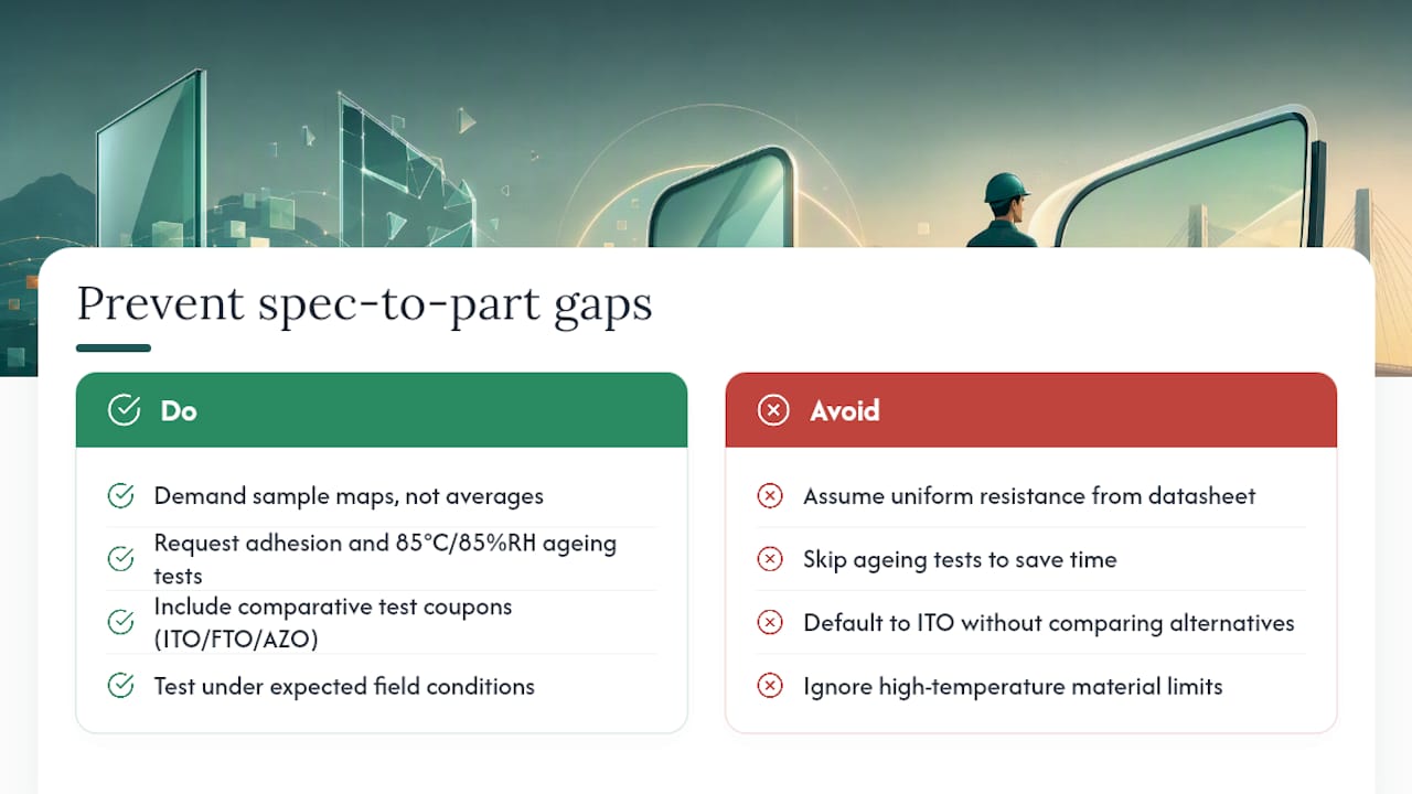
That is the real argument for demanding sample maps rather than averaged figures, and for treating adhesion and environmental ageing tests as standard requests rather than optional extras reserved for aerospace work. A touch panel destined for a factory floor faces thermal cycling and humidity that a lab bench sample never sees. Skipping the 85°C/85% RH ageing test to save a week on the quote almost always costs more time later, when a batch of parts starts delaminating in the field six months after installation.
The other underestimated point is how often the “obvious” material choice is the wrong one. ITO gets specified by habit because it is the default TCO everyone learned first, but a project running at 500°C process temperatures has no business anywhere near an ITO layer when FTO exists precisely for that case. Indium price swings have made this decision less theoretical over the past several years. Engineers who build comparative test coupons into an early design review, ITO against FTO or AZO on the same substrate, catch this mismatch before it becomes a redesign.
— Alexandra
Sources
For deeper reference, consult the transparent conducting oxide review, TCF deposition methods paper, and supplier spec sheets cited throughout this guide, alongside ASTM D1003 for haze testing.
- Transparent conducting oxides review — PMC
- A Review of Transparent Conducting Films (TCFs): Prospective ITO and AZO Deposition Methods and Applications
- itoCoatedGlassSub.pageTitle | GINECHIP™
- Low-temperature deposition of transparent and conductive coatings – Fraunhofer IOF
- ITO Coated Glass Supplier | Stanford Advanced Materials