
Glass has long carried an undeserved reputation as a fragile, impractical material for demanding applications. In electronics manufacturing, that reputation is increasingly at odds with reality. Glass is now central to advanced packaging, high-frequency interconnects, precision displays, and sensor platforms. Yet adopting glass successfully requires far more than specifying the right substrate. Design engineers and procurement specialists must navigate a nuanced landscape of material properties, process constraints, and reliability risks. This article addresses all of those considerations with clarity and practical precision.
Table of Contents
- Glass in electronics: Beyond fragility
- Performance advantages and engineering applications
- Reliability and manufacturing constraints
- Procurement and design integration: What specialists must know
- Our perspective: Glass delivers, but process and reliability remain king
- Explore advanced glass solutions for next-generation electronics
- Frequently asked questions
Key Takeaways
| Point | Details |
|---|---|
| Glass boosts performance | Low dielectric loss and flatness drive miniaturisation and accuracy in electronics. |
| Reliability is critical | Process control and stress management are essential to prevent failure in glass-core devices. |
| Procurement requires new checks | Glass adoption mandates nuanced process validation for durability and manufacturing yield. |
| Collaboration is key | Early-stage cooperation between design and supply ensures optimal glass integration and reliability. |
Glass in electronics: Beyond fragility
Having raised the question of glass’s suitability, it is vital to explore the properties that drive its adoption in electronics. The instinct to dismiss glass as too brittle for demanding applications underestimates how thoroughly its characteristics align with the requirements of modern electronic design. When engineers look closely, several properties stand out as genuinely differentiated compared to organic and polymer-based alternatives.
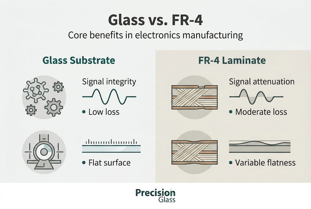
Dielectric performance is perhaps the most significant. Glass offers a low dielectric constant and low dielectric loss tangent, which means signal integrity is preserved even at millimetre-wave frequencies. As electronic devices push into higher frequency bands for 5G, radar, and sensing applications, this becomes a critical selection criterion rather than a nice-to-have feature. High-frequency interconnects benefit specifically from glass’s low dielectric loss and its tunable coefficient of thermal expansion (CTE), making it suitable for next-generation packaging architectures.
Thermal expansion compatibility matters because electronic assemblies experience repeated thermal cycling during manufacture and service. When the CTE of the substrate mismatches that of the die, solder joints, or deposited metal layers, stress accumulates and failures follow. Glass can be engineered to closely match silicon’s CTE, reducing interfacial stress significantly compared to standard organic laminates. This is not a marginal improvement. It is often the deciding factor in long-lifecycle, high-reliability applications such as aerospace avionics and medical implantables.
Dimensional stability and flatness are equally important, particularly for display and sensor applications. Glass provides a surface flatness that is difficult to match with polymer-based substrates. This translates directly into display accuracy, lithography precision, and the repeatability needed for automated assembly. You can explore the specific display glass benefits in detail, but the short version is that flatness tolerances achievable in glass are simply not replicable in organic alternatives at scale.
Beyond these headline properties, glass offers:
- Chemical resistance, which simplifies wet-process cleaning steps during fabrication without substrate degradation
- Optical transparency, enabling integration of optical sensing directly into glass-core structures
- Electrical insulation, providing excellent isolation between conducting layers at high voltages
- Surface smoothness, critical for fine-pitch metal deposition and lithographic patterning
Reviewing the broader range of technical glass types clarifies how different compositions address different combinations of these properties, whether the priority is optical clarity, thermal stability, or mechanical strength.
“Glass is not simply a passive substrate. In advanced electronics, it is an active participant in electrical, thermal, and mechanical performance. Choosing it demands engineering rigour from the outset.”
The manufacturing industry cases from electronics and semiconductor sectors illustrate how firms that treated glass as a direct swap for organic laminates encountered preventable failures, whilst those who invested in process validation from the design stage achieved reliable, high-performing results.
Performance advantages and engineering applications
With the foundational properties established, the next step is understanding how glass transforms electronic component design. The most prominent application driving interest in glass substrates today is Through-Glass Via (TGV) technology. TGVs are precisely formed vertical interconnects drilled or etched through glass substrates, filled with copper or other conductors, enabling three-dimensional stacking and integration of chips, sensors, and passive components within extremely compact packages.
TGV technology is used for next-generation packaging owing to low dielectric loss and superior CTE compatibility, though it also introduces well-documented failure risks from thermal stress. Understanding those risks upfront, rather than discovering them during qualification, separates teams that succeed with glass from those that do not.
The performance advantages of glass-based electronics extend across several application classes:
| Property | Glass substrate | Organic laminate (FR-4) |
|---|---|---|
| Dielectric loss at 10 GHz | Very low | Moderate to high |
| CTE (ppm/°C) | 3 to 6 (adjustable) | 12 to 18 |
| Surface flatness | Excellent | Moderate |
| Optical transparency | Yes (borosilicate, etc.) | No |
| Crack sensitivity | High | Low |
| Chemical resistance | High | Moderate |
| Cost at volume | Moderate to high | Low |
This table illustrates the clear performance lead glass holds in high-frequency and precision applications, alongside the equally clear trade-off in brittleness and cost. The decision to use glass is therefore not simply a performance decision. It is a full system-level commitment to process control and qualification.
For displays and camera modules, glass’s flatness enables sub-micron lithographic precision over large panel areas. For RF and microwave packaging, its dielectric properties reduce insertion loss and support densely packed antenna-in-package designs. For medical sensors, its biocompatibility and optical transparency open possibilities that silicon alone cannot achieve.

When evaluating sources and approaching optimising glass sourcing, design engineers should prioritise suppliers who understand not just the material but the downstream assembly processes that glass will encounter. This includes reflow soldering, wire bonding, and underfill dispensing, all of which impose thermal and mechanical loads on glass components.
For optical systems and sensor integration, optical glass components represent a distinct category where surface quality, refractive index uniformity, and transmission properties are specified with extreme precision. These are not commodity items, and procurement must reflect that reality.
Pro Tip: Identify the maximum thermal gradient your assembly process imposes on the glass substrate before finalising your design. Residual thermal stress from reflow or bonding operations is a leading cause of early-life failures in TGV-based packages. Designing around that constraint from the outset avoids costly late-stage redesigns.
Reliability and manufacturing constraints
Though glass delivers substantial benefits, engineers must also navigate key process and reliability limitations. This is where many glass adoption programmes encounter difficulty. The brittleness of glass is real, and it manifests in specific, predictable failure modes that demand rigorous process control.
Glass adoption introduces reliability failure modes driven by thermal stress mismatch, copper-to-glass interfacial behaviour, and crack sensitivity. Each of these failure modes is manageable, but none can be managed passively. They require active engineering decisions at every stage from design through to final test.
The TGV process-control requirements are specific and non-trivial. They include crack risk at via edges, critical-dimension control across the top, waist, and bottom of each via, thickness uniformity requirements across the substrate panel, and residual stress management throughout thermal processing steps.
| Reliability risk | Root cause | Mitigation approach |
|---|---|---|
| Edge cracking at vias | Stress concentration during drilling or etching | Optimise laser or wet-etch parameters; control sidewall profile |
| Cu-glass delamination | CTE mismatch under thermal cycling | Match Cu fill process to glass CTE; use stress-relief structures |
| Panel-level warpage | Non-uniform residual stress post-anneal | Controlled annealing profiles; panel fixturing during processing |
| Crack propagation | Pre-existing surface flaws under tensile stress | Incoming substrate inspection; edge chamfering where applicable |
Managing these risks in practice requires a structured approach. The following steps represent a reliable methodology for teams integrating glass-core electronics into a production process:
- Define your thermal envelope before material selection. Confirm the maximum and minimum temperatures the glass will experience during manufacture and service life.
- Qualify via formation processes separately from substrate qualification. Laser drilling, CO₂ etching, and wet chemical etching each produce different sidewall profiles and stress states.
- Characterise residual stress at each major processing step, including after metallisation, plating, and annealing, using techniques such as Raman spectroscopy or polarimetry.
- Implement dimensional inspection for via profiles across the full panel, not just at the centre, to capture any edge-to-edge variation introduced by your process equipment.
- Conduct thermal cycling qualification representative of your end-use environment before committing to production volumes.
For applications in demanding sectors, the constraints are no less stringent. The aerospace glass constraints page outlines how similar principles apply to components where failure is simply not an option. Aerospace and defence programmes routinely apply these structured qualification approaches, and electronics manufacturers can draw directly on those methodologies.
Practical quality control guidance from manufacturing specialists reinforces the message: in-process measurement and process characterisation are not optional extras. They are the mechanisms by which glass’s performance potential is actually realised rather than compromised.
Procurement and design integration: What specialists must know
Understanding manufacturing constraints leads directly into effective procurement and design strategies. Glass adoption is not just a material swap. It introduces process control and reliability constraints covering crack initiation, via profile and copper filling integrity, and residual stress evolution that must be managed throughout the manufacturing cycle. Procurement specialists who treat glass as a commodity purchase risk significant programme disruption.
The procurement questions you ask a glass supplier are fundamentally different from those you would ask a standard laminate supplier. Consider the following areas before committing to a supply relationship:
- Substrate thickness uniformity: What are the tolerance bands across a full panel, and how are they verified in production?
- Via profile specifications: Can the supplier demonstrate consistent top, waist, and bottom diameter control across the panel at your required pitch?
- Residual stress characterisation: Does the supplier provide stress data from the production lot, or only from qualification samples?
- Surface quality and scratch/dig specifications: How are incoming substrates inspected, and what is the reject rate at acceptance?
- Traceability and lot documentation: Can the supplier provide full material traceability from melt to finished substrate?
- Lead times for custom compositions: If your design requires a specific CTE or optical property, what is the development and qualification timeline?
These questions reflect the depth of engagement that glass procurement requires. Specialists working across medical glass terminology and display glass integration will recognise that the vocabulary and the technical requirements shift significantly between sectors, even when the base material is ostensibly the same.
Design integration itself demands close alignment between the glass supplier and the assembly house. Reflow profiles, board-level underfill materials, and fixture designs all interact with the glass substrate’s mechanical and thermal properties. The earlier in the design cycle you bring your supplier into those discussions, the less likely you are to encounter late-stage surprises.
A useful production quality guide for manufacturing teams confirms that process validation documentation produced collaboratively between supplier and customer consistently outperforms documentation produced by either party independently. This collaborative approach is not merely best practice. In glass electronics, it is a prerequisite for reliable yield.
Pro Tip: Request sample panels from any candidate supplier and run your full assembly thermal profile against them before placing a volume order. Glass from different suppliers, even at nominally identical specifications, can behave differently under your specific process conditions.
Our perspective: Glass delivers, but process and reliability remain king
We have worked with design engineers and procurement specialists across a wide range of industries who initially approached glass substrates with enthusiasm for the performance numbers and scepticism about the process complexity. In our experience, both reactions are justified, and neither should override the other.
The reliability failure modes documented in technical literature, namely thermal stress mismatch, copper-to-glass interfacial failure, and crack sensitivity, are not theoretical concerns. They are real failure mechanisms that have terminated otherwise well-conceived programmes. The temptation to chase performance specifications without investing equally in process validation is understandable but costly.
Our position is straightforward: glass delivers genuine, measurable advantages in the right applications. But the material’s performance potential is only realised when process control and reliability qualification receive the same investment as material selection. Reaching for optimising glass sourcing strategies early in the programme is as important as choosing the right glass composition.
Design teams that allocate budget for process characterisation upfront consistently achieve better outcomes than those who defer it to late-stage qualification. That is not a sales proposition. It is what the evidence consistently shows.
Explore advanced glass solutions for next-generation electronics
For design engineers and procurement specialists ready to move from evaluation to action, we offer a broad portfolio of precision-engineered glass solutions tailored to the exact demands of modern electronics manufacturing.

Our technical glass portfolio covers a wide range of compositions, dimensions, and surface specifications suited to high-frequency packaging, display integration, and optical sensing. For programmes requiring the highest reliability standards, our aerospace glass solutions provide a reference point for what rigorous qualification and process control look like in practice. If you are working through sourcing decisions, our resources on optimising glass sourcing will give you a practical framework. We welcome early engagement, because in glass electronics, early collaboration consistently produces the best outcomes.
Frequently asked questions
What are the main benefits of glass in electronic devices?
Glass provides low dielectric loss and tunable CTE compatibility, making it highly suitable for high-frequency interconnects, alongside superior flatness for precision display and sensor applications.
Why is process control important when adopting glass for electronics?
Glass substrates require precise management of crack risk and dimensional control across via top, waist, and bottom profiles, as well as residual stress throughout thermal processing, to avoid brittle failure and maintain yield.
How does glass compare to organic laminates like FR-4 in electronic applications?
Glass offers significantly better high-frequency performance and thermal stability, but its brittle via design logic makes stress and edge control far more critical than in organic laminates, requiring substantially more rigorous process qualification.
Can glass-core electronics fail if reliability processes are overlooked?
Yes. Prolonged annealing can generate residual tensile stress that leads directly to glass cracking, and broader thermal stress mismatch risks can quickly outweigh the performance gains glass would otherwise deliver.
Recommended
- Display glass explained: precision, performance and industry solutions – Precision Glass
- How to optimise glass sourcing for precision: 5 key steps – Precision Glass
- Top glass solutions for aerospace: strength, clarity, precision – Precision Glass
- Medical glass terminology explained for device engineers – Precision Glass