
Thin film coating is defined as the application of a material layer ranging from fractions of a nanometre to approximately 1 micrometre in thickness onto a substrate, modifying its surface properties without altering its bulk characteristics. This process sits at the heart of precision engineering across optics, electronics, aerospace, and defence. Techniques such as Physical Vapor Deposition (PVD) and Chemical Vapor Deposition (CVD) give engineers the ability to tailor surface behaviour with nanometre-level accuracy. Understanding what is thin film coating, and how it differs from thicker protective coatings, is the first step towards specifying the right process for your application.
What thickness and materials qualify as thin film coatings?
A thin film is defined as any layer thinner than approximately 1 micrometre. Layers exceeding that threshold are classified as conventional coatings rather than thin films. This distinction matters because the physical and optical behaviour of a film changes fundamentally at the nanoscale.
The materials used span a wide range of chemical families. Common thin film materials include metals such as aluminium and copper, metal oxides such as titanium dioxide, nitrides such as titanium nitride, and advanced nanocomposites engineered for durability. Material selection is driven entirely by the required optical, electrical, or mechanical outcome.

A key engineering principle is that thin films decouple bulk and surface properties. A titanium substrate can retain its structural strength while a titanium nitride thin film on its surface delivers exceptional hardness and wear resistance. That separation of functions is what makes thin film technology so powerful for high-performance components.
| Thickness range | Typical materials | Primary properties |
|---|---|---|
| 1–10 nm | Metal oxides, nitrides | Barrier layers, seed layers |
| 10–100 nm | Aluminium, silicon dioxide | Anti-reflective, conductive |
| 100–500 nm | Titanium dioxide, titanium nitride | Optical filtering, wear resistance |
| 500 nm–1 µm | Nanocomposites, carbides | Hard coatings, corrosion protection |
What are the main deposition methods used in thin film coating?
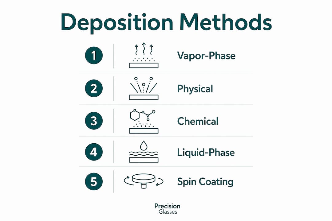
Industrial thin film deposition divides into two broad families: vapor-phase and liquid-phase techniques. Vapor-phase methods are preferred for semiconductors and optical components because they deliver high purity and film density. Liquid-phase methods offer cost advantages for specific industrial and flexible electronics applications.
Vapor-phase techniques
PVD encompasses magnetron sputtering and thermal evaporation. In sputtering, a target material is bombarded by ions, ejecting atoms that travel to the substrate and condense as a film. Evaporation heats the source material until it vaporises, then deposits onto a cooled substrate. Both methods suit precision glass fabrication where optical-grade surface quality is non-negotiable.
CVD introduces reactive gases into a chamber where they decompose and react on the substrate surface, forming a solid film. Atomic Layer Deposition (ALD) is a variant of CVD that deposits material one atomic layer at a time, giving exceptional thickness control for the most demanding applications.
Liquid-phase techniques
Spin coating, dip coating, and electroplating are the principal liquid-phase routes. Spin coating deposits a liquid precursor onto a rotating substrate; centrifugal force spreads the film uniformly before it cures. Dip coating draws a substrate through a liquid bath at a controlled speed. Electroplating uses an electrical current to deposit metal ions from solution. These methods complement vapor-phase techniques by offering scalability for large-area or flexible substrates.
Pro Tip: Substrate preparation is as critical as the deposition method itself. A film deposited on a contaminated surface will fail regardless of process quality. Specify your cleaning protocol before you specify your deposition equipment.
| Method | Mechanism | Typical materials | Equipment complexity | Common applications |
|---|---|---|---|---|
| Magnetron sputtering | Ion bombardment of target | Metals, oxides, nitrides | High | Optical coatings, semiconductors |
| Thermal evaporation | Resistive or e-beam heating | Metals, simple oxides | Medium | Reflective coatings, electronics |
| CVD | Gas-phase chemical reaction | Silicon nitride, oxides | High | Microelectronics, wear coatings |
| ALD | Sequential self-limiting reactions | Oxides, nitrides | Very high | Advanced semiconductors, MEMS |
| Spin coating | Centrifugal spreading of liquid | Polymers, sol-gel oxides | Low | Flat panel displays, photoresists |
| Electroplating | Electrochemical deposition | Copper, nickel, gold | Low to medium | PCBs, decorative coatings |
How do thin film coatings enhance performance in optics, electronics, and industrial applications?
Thin film coatings enhance devices across aerospace, defence, telecommunications, medical diagnostics, and consumer electronics. They deliver anti-reflective layers, wear-resistant surfaces, conductive paths, and low-emissivity barriers within a single micrometre of material. The functional range is extraordinary relative to the physical scale involved.
Optical applications
Optical thin films exploit interference between light waves reflected at each layer boundary. By controlling film thickness to within the 200–1,000 nm range, engineers can manage wavelength filtering with high precision. Anti-reflective coatings on camera lenses, laser optics, and medical imaging systems all rely on this principle. The refractive index of each layer is chosen to create constructive or destructive interference at specific wavelengths. You can explore how these principles apply to precision optical components in demanding sectors.
Electronics applications
Thin films form the conductive and insulating layers inside every modern semiconductor device. Copper thin films create interconnects between transistors; silicon dioxide films act as gate dielectrics. These layers enable device miniaturisation by delivering electrical function within nanometre-scale geometries. Reliability depends directly on film uniformity and adhesion quality.
Industrial and protective applications
The benefits of thin film coating in industrial contexts centre on surface durability. Key performance gains include:
- Wear resistance: Titanium nitride and diamond-like carbon (DLC) coatings extend tool life significantly in machining and forming operations.
- Corrosion protection: Oxide and nitride films act as diffusion barriers, preventing moisture and reactive gases from reaching the substrate.
- Low friction: DLC and molybdenum disulphide films reduce friction in bearings, gears, and sliding contacts without lubrication.
- Thermal management: Low-emissivity coatings on glass control heat transfer in architectural and automotive glazing. Industrial thin film applications in glazing demonstrate how a sub-micrometre layer can transform thermal performance at scale.
- Biocompatibility: Titanium dioxide and hydroxyapatite films on medical implants promote osseointegration and resist biological fouling.
What are key challenges and quality control considerations in thin film coating?
Surface contamination at the atomic scale causes the most common thin film failures. Adhesion failure, delamination, and pinholes all originate from inadequate substrate preparation. Ultrasonic cleaning, plasma cleaning, and ion bombardment are the standard methods for achieving the surface energy required for reliable bonding.
Geometry presents a separate challenge. PVD is a line-of-sight process, meaning it cannot coat recesses, undercuts, or complex 3D shapes uniformly without specialised fixturing and substrate rotation. CVD and ALD deposit conformally, following the substrate geometry regardless of complexity. Choosing the wrong method for a complex part geometry leads to uneven film thickness and localised performance failures.
Thickness control is the third critical variable. Real-time monitoring during deposition uses quartz crystal microbalances (QCM) or optical thickness sensors to track film growth. Small deviations in an optical coating can cause complete failure of its intended wavelength function. Precision glass components destined for defence or medical optics demand monitoring throughout the entire deposition run, not just at the end. Precision Glasses integrates quality assurance measures at every stage of the fabrication process to address exactly these risks.
Key quality control considerations for engineers:
- Specify substrate cleanliness to a defined surface energy value, not just a visual standard.
- Match the deposition method to the substrate geometry before specifying materials.
- Use in-situ QCM or optical monitoring for any optical coating where thickness tolerance is below 10 nm.
- Define acceptable pinhole density and adhesion strength as measurable acceptance criteria.
- Validate coating performance on representative test substrates before full production runs.
Pro Tip: Integrate coating requirements into the component design phase, not as an afterthought. Film stress, thermal expansion mismatch, and edge coverage all depend on geometry decisions made at the design stage. Reviewing component design considerations early prevents costly redesigns later.
How does thin film coating compare to thick film coating?
Thin and thick films differ primarily by the 1 micrometre thickness boundary. Thin films are used for precision surface engineering where the substrate geometry must not change. Thick films, typically applied by screen printing, thermal spray, or chemical plating, add measurable physical bulk and suit applications where structural protection or electrical conductivity at scale is the priority.
Thin films deliver optical and electronic functions that thick films physically cannot. A thick film cannot produce interference-based anti-reflective behaviour because its physical scale overwhelms the wavelength of light. Conversely, a thin film cannot provide the mechanical protection of a 50-micrometre thermal spray coating on a turbine blade.
| Criterion | Thin film (<1 µm) | Thick film (>1 µm) |
|---|---|---|
| Thickness control | Nanometre precision | Micrometre to millimetre |
| Optical function | Anti-reflective, filtering, interference | Absorptive, bulk reflective |
| Substrate geometry change | Negligible | Measurable |
| Deposition methods | PVD, CVD, ALD, spin coating | Thermal spray, screen printing, plating |
| Typical applications | Optics, semiconductors, precision tools | Turbine blades, PCB conductors, wear plates |
| Cost per unit area | Higher | Lower |
The decision between thin and thick film is driven by functional requirement, not cost alone. Where nanometre-scale precision determines product performance, thin film deposition is the only viable route.
Key takeaways
Thin film coating is the most precise method available for engineering surface properties without altering substrate geometry, making it indispensable for optics, electronics, and high-performance industrial components.
| Point | Details |
|---|---|
| Thickness defines the category | Films below 1 µm are thin films; above that threshold they are conventional coatings with different properties. |
| Method must match geometry | PVD suits flat or simple substrates; CVD and ALD are required for conformal coverage of complex 3D parts. |
| Substrate preparation is critical | Atomic-scale contamination causes delamination and pinholes; plasma or ion cleaning is the standard solution. |
| Real-time monitoring protects quality | QCM and optical sensors during deposition prevent thickness deviations that would cause optical coating failure. |
| Thin vs thick film is a functional choice | Optical and electronic functions require thin films; structural protection applications suit thick film methods. |
Thin film coating in precision manufacturing: my perspective
The conversation around thin film technology in manufacturing has shifted noticeably over the past several years. Engineers who once treated coating as a finishing step now specify it at the design stage, and that change reflects a genuine maturation in how the industry understands surface engineering.
What I find most underappreciated is the cost of getting the method selection wrong. PVD and CVD can produce superficially similar coatings, but their process intensity and cost profiles diverge sharply. Specifying ALD for a component that could be coated by magnetron sputtering adds expense without adding value. The reverse error, choosing sputtering for a complex 3D geometry, produces a coating that fails in service. Neither mistake is obvious until it is expensive.
The sectors I see pushing thin film technology hardest right now are medical optics and defence. Both demand coatings that perform reliably under conditions that cannot be replicated in standard qualification testing. That pressure is driving investment in real-time process monitoring and tighter substrate preparation protocols. Engineers entering these sectors need to treat coating knowledge as a core competency, not a supplier problem to delegate.
My honest view is that the gap between what thin film technology can deliver and what most manufacturing teams actually specify remains wide. Closing that gap starts with understanding the physics, not just the product catalogue.
— Alexandra
Precision Glasses: thin film expertise for critical applications

Precision Glasses designs and fabricates custom glass components for defence, aerospace, medical devices, automotive, and electronics applications where coating performance is as critical as substrate quality. Our manufacturing process covers the full chain from precision glass design through to final quality assurance, with meticulous attention to surface preparation, deposition specification, and acceptance testing. We work with engineers at the design stage to align coating requirements with component geometry before fabrication begins. Explore our full range of precision engineered glass solutions to see how we support the sectors that demand the highest surface performance standards.
FAQ
What is thin film coating in simple terms?
Thin film coating is the deposition of a material layer thinner than 1 micrometre onto a substrate to change its surface properties, such as reflectivity, hardness, or conductivity, without altering the underlying material.
What materials are used in thin film coatings?
Common materials include metals such as aluminium and copper, metal oxides such as titanium dioxide, nitrides such as titanium nitride, and nanocomposites. Material choice depends on the required optical, electrical, or mechanical properties.
What is the difference between PVD and CVD in thin film deposition?
PVD is a line-of-sight process suited to flat or simple geometries, while CVD deposits conformally and covers complex 3D shapes uniformly. Both produce high-quality films, but they differ significantly in cost and process complexity.
How is thin film thickness controlled during deposition?
Quartz crystal microbalances and optical thickness sensors monitor film growth in real time during deposition. This is particularly critical for optical coatings where thickness deviations of even a few nanometres can cause functional failure.
Where are thin film coatings used in industry?
Thin film coatings are used in optical lenses, semiconductor devices, medical implants, aerospace components, cutting tools, and architectural glazing. They deliver anti-reflective, wear-resistant, conductive, and corrosion-protective functions across these sectors.