Across defence electronics, medical imaging, advanced packaging, and optical systems, engineers and procurement managers routinely specify “glass substrates” yet frequently mean entirely different things. A display engineer’s substrate is flat panel glass measured in square metres. A semiconductor packaging specialist’s substrate is a precision wafer measured in microns of dielectric loss. A MEMS fabricator’s substrate is a chemically resistant platform for micro-etching. The same two words, four wildly divergent specifications. That gap between shared terminology and sector-specific reality causes real procurement errors, costly re-qualification cycles, and programme delays that could be avoided with a clearer, more rigorous approach from the outset.
Table of Contents
- What is a glass substrate?
- Glass substrate functions and engineering requirements
- Processing methods and defect control
- Choosing glass substrates for precision applications
- The uncomfortable truth about glass substrate selection
- Connect with precision glass solutions
- Frequently asked questions
Key Takeaways
| Point | Details |
|---|---|
| Glass substrate baseline | A glass substrate is a glass sheet or wafer serving as a structural platform with electrical and optical properties. |
| Sector-specific requirements | Electronics, optics, and medical applications each demand tailored specifications for glass substrates. |
| Process and defect risk | Cracks and flaws during fabrication or handling can severely impact substrate reliability and yield. |
| Procurement benchmarks | Effective procurement includes edge, surface, and processing tolerances beyond simple material specs. |
| Precision solution sourcing | Aligning substrate selection to both application and yield expectations is vital for performance. |
What is a glass substrate?
At its most fundamental level, a glass substrate is a glass-based panel or wafer used as the base platform providing mechanical support and electrical insulation for structures built upon it. It is the foundation layer. Everything else, whether deposited circuits, optical coatings, microfluidic channels, or sensor arrays, relies on it for dimensional stability, structural integrity, and predictable physical properties.
The core attributes that make glass attractive as a substrate are well established. Glass offers excellent electrical insulation, a low and tuneable coefficient of thermal expansion, high stiffness relative to its weight, and optical clarity across a wide range of wavelengths. It is chemically inert under many process conditions and can be polished to sub-nanometre surface roughness levels. These properties are consistent across sectors. What changes is which properties matter most and how tightly they must be controlled.

The term “glass substrate” is application-dependent, with requirements diverging substantially for electronics, MEMS, and optical or display contexts. Understanding glass engineering basics is therefore the necessary starting point before any meaningful specification work begins.
| Sector | Primary substrate form | Typical thickness | Key property |
|---|---|---|---|
| Advanced electronics packaging | Wafer or panel | 100 to 300 µm | Dielectric loss, TGVs |
| Display and HMI | Large panel | 0.5 to 1.1 mm | Flatness, optical clarity |
| Medical devices and MEMS | Small wafer or chip | 200 to 500 µm | Chemical resistance |
| Optical systems and defence | Polished plate | 1 to 10 mm | Surface figure, transmission |
| Automotive dashboards | Formed panel | 1.6 to 3 mm | Impact resistance, clarity |
“The definition of a glass substrate is only complete when you add the sector context. A datasheet that stops at chemical composition and thickness is incomplete from an engineering standpoint.”
This table alone illustrates why a single purchasing description referencing “glass substrate, 200 µm, borosilicate” is insufficient. Thickness and material class are starting points, not complete specifications.
Glass substrate functions and engineering requirements
With the definition in hand, let’s explore the functions and diverse engineering requirements that shape glass substrate solutions for different industries.
Mechanical role. The substrate must maintain dimensional stability throughout its entire process lifetime. That means surviving thermal cycles during deposition, chemical baths during etching, and mechanical stress during dicing, handling, and assembly. Edge quality is particularly critical. A chipped or micro-cracked edge on a glass substrate is not a cosmetic issue. It is a fracture initiation site that can propagate under subsequent thermal or mechanical loading and cause catastrophic failure mid-process.
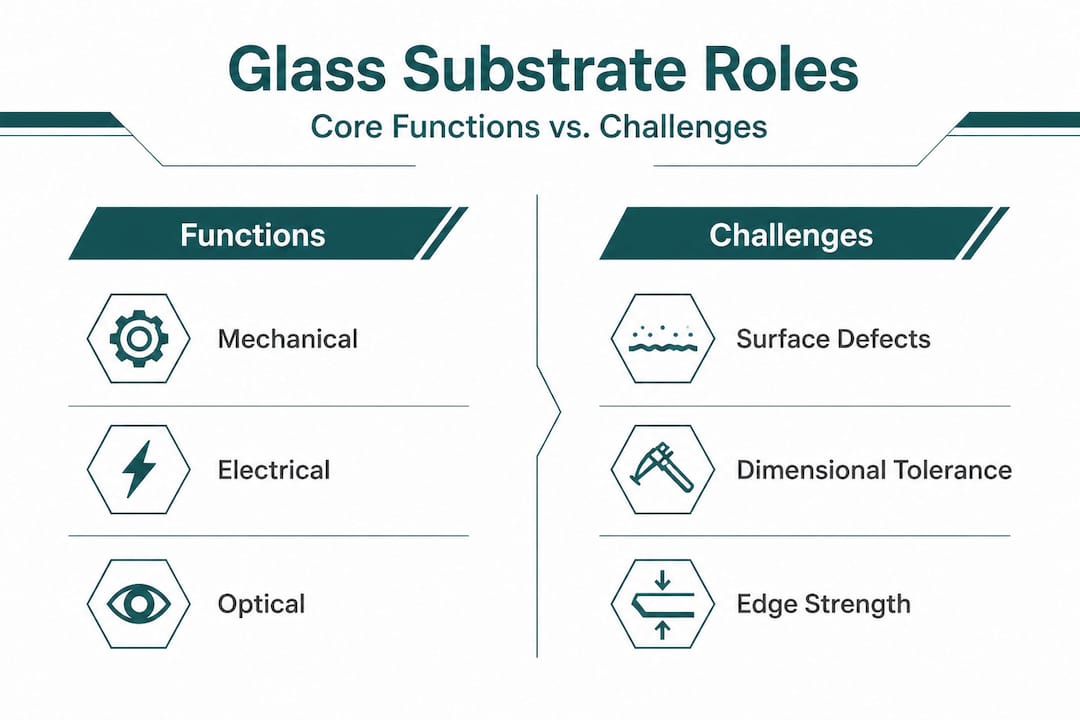
Electrical role. In electronic packaging, glass substrates offer dielectric behaviour that supports high-frequency signal integrity, enabling fine-pitch interconnects and through-glass via (TGV) formation. Dielectric loss tangent, resistivity, and permittivity must all be quantified and tightly controlled for RF and millimetre-wave packaging applications. This is quite different from a display application where electrical insulation is necessary but high-frequency signal transmission is irrelevant.
Optical role. For defence optics, medical imaging, and automotive heads-up displays, the substrate must transmit specific wavelength ranges with minimal distortion. Surface flatness, measured in waves or nanometres of deviation, directly affects optical performance. A substrate that is perfectly flat to within one micrometre may be sufficient for a display but entirely inadequate for a laser or interferometric application requiring flatness to within a fraction of a wavelength.
Qualification requirements differ for electronics (focusing on TGVs and dielectric loss), optical applications (flatness and transmission), and MEMS (chemical resistance and etch uniformity). Aligning your qualification protocol to the correct category before procurement begins saves substantial time and cost.
Key engineering benchmarks by sector:
- Electronics and packaging: Dielectric constant below 5.5 at 10 GHz, loss tangent below 0.005, via pitch capability below 100 µm
- Medical and MEMS: Hydrofluoric acid resistance, particulate cleanliness class, biocompatibility certification where applicable
- Optical and defence: Surface flatness better than λ/10, scratch-dig specification per MIL-PRF-13830, transmission uniformity across full aperture
- Automotive: Impact resistance to ECE R43 or equivalent, anti-glare treatment compatibility, dimensional tolerance for formed shapes
Our glass fabrication processes are tailored to meet these distinct sector benchmarks, and our display glass solutions illustrate how application-specific engineering translates into production-ready components.
Pro Tip: When specifying glass substrates, always list the primary function first in your procurement document. Is the substrate primarily mechanical, electrical, or optical? This hierarchy drives every downstream specification choice, from material grade to surface finish to edge treatment.
Processing methods and defect control
Understanding what glass substrates must do, let’s turn to how they’re made and what can go wrong in the process, directly impacting your procurement risks.
Glass substrate fabrication is not a single process. It is a sequence of interdependent steps, each of which introduces its own defect risk. For advanced applications such as TGV formation, the fabrication flow includes laser modification, selective etching, metallisation, and planarisation, with crack defects in glass representing critical reliability threats if process control is not rigorously maintained.
A typical precision substrate processing sequence runs as follows:
- Incoming material inspection. Verify bulk glass properties: composition, inclusion count, internal strain birefringence, and dimensional conformance to drawing.
- Cutting and shaping. Laser scribing, water-jet cutting, or mechanical dicing. Each method introduces different edge stress profiles. Laser processes offer cleaner edges but require careful parameter control to avoid sub-surface micro-cracking.
- Grinding and lapping. Brings the substrate to near-final thickness and flatness. Abrasive selection and lubrication management are critical to avoid surface contamination that resists subsequent cleaning.
- Polishing. Chemical mechanical polishing (CMP) or pitch polishing achieves surface roughness specifications. For optical applications, this stage can represent the majority of value-add time.
- Cleaning and inspection. Ultrasonic cleaning, optical profilometry, and automated defect scanning. Any unacceptable substrate is quarantined here, not at final assembly.
- Functional processing. Deposition of coatings, via drilling, metallisation, or bonding preparation, depending on the application.
Glass is brittle and highly sensitive to surface flaws, which means procurement definitions must include fracture-mechanics considerations and explicit handling requirements. This is a point that is consistently underweighted in early-stage procurement discussions.
A substrate that passes optical inspection but has been handled without edge protection during transit can fail during its first thermal cycle in production. The fracture mechanics here are well understood: a surface flaw of 10 µm depth can reduce the effective strength of a glass substrate by more than 50% compared to a flaw-free surface. Specifying edge chamfer dimensions, packaging method, and permitted handling temperatures is not over-engineering. It is essential reliability management.
Pro Tip: Include explicit edge specification and packaging requirements in your purchase order, not just in a verbal briefing. If edge chamfer radius, maximum chip size, and transit packaging method are not on the drawing or purchase document, they cannot be inspected or enforced at goods-in.
Working with our team on advanced glass specifications and reviewing guidance on optimising glass sourcing can help you build procurement documents that capture these critical parameters from the outset.
Choosing glass substrates for precision applications
As we’ve seen, processing and defect control shape the risks. Now let’s distil practical guidance for sourcing the right glass substrate for precise applications, especially for high-stakes sectors.
The central question when specifying a glass substrate for a precision application is not “what is available?” It is “what does this substrate need to do, and under what conditions must it survive?” Starting from functional requirements and working backwards to material and process specification produces far more reliable outcomes than starting from a material datasheet and hoping the application fits.
For ultrathin substrates below 200 µm, mechanical strength and yield depend heavily on cutting and handling conditions, and procurement teams must specify edge and handling tolerances alongside thickness. Ultrathin glass is increasingly common in foldable displays, wearable medical sensors, and advanced packaging interposers, and it requires an entirely different handling infrastructure compared to standard display glass. Edge bead reinforcement, vacuum pickup tooling, and dedicated carrier trays are all necessary investments that must be factored into programme costs.
In high-frequency electronics packaging, the substrate advantage is defined by low dielectric loss, precise flatness for fine-pitch interconnects, and rigorous yield inspection. For millimetre-wave applications at frequencies above 40 GHz, a 10% variation in dielectric constant across a substrate panel can meaningfully degrade signal integrity at the system level. Yield inspection must therefore include electrical characterisation, not just visual or dimensional checks.
Practical procurement benchmarks to include in specifications:
- Thickness tolerance: specify as ± value, not just nominal
- Flatness: define bow and warp separately, with measurement aperture stated
- Surface roughness: specify Ra and Rq, with measurement area and cut-off wavelength
- Edge quality: maximum chip size, chamfer dimensions, and method of inspection
- Cleanliness: maximum particle size and count per unit area before packaging
- Packaging: humidity-controlled, nitrogen-purged, or vacuum-sealed as appropriate to application
For medical device applications, add biocompatibility evidence requirements (ISO 10993 testing data), sterilisation compatibility (autoclave, gamma, or EtO), and cleanroom handling certification to this list.
For defence and aerospace, material traceability documentation, compliance to relevant military or aerospace standards, and evidence of lot-specific testing are typically mandatory rather than optional.
Reviewing glass in electronics procurement provides further sector-specific guidance on translating these requirements into practical purchasing language.
The uncomfortable truth about glass substrate selection
The industry has a tendency to treat glass substrate selection as primarily a materials science problem. Engineers pore over datasheets, compare coefficients of thermal expansion to three decimal places, and debate the merits of borosilicate versus aluminosilicate compositions at length. Yet the most common root causes of glass substrate-related programme failures we encounter are not compositional at all. They are process and handling failures that occurred because those risks were not specified, inspected, or managed.
Edge micro-cracks introduced by a non-compliant dicing process. Substrates warped by a polishing step that ran too hot. Contamination trapped under a deposited layer because cleaning was not validated for that surface finish. These failures are entirely predictable if the right questions are asked during qualification. The problem is that procurement teams are often not asking those questions because the focus is on material properties rather than process capability.
Our view, informed by years of working with engineers in defence, medical, and advanced electronics programmes, is that specification best practices must give equal weight to process control parameters and yield inspection criteria as they do to material composition. A supplier who can demonstrate process capability data, in-process inspection records, and lot-level yield statistics is more valuable than one who offers a marginally better dielectric constant with no process transparency.
The second uncomfortable truth is that many procurement teams still treat glass substrates as a commodity purchase, driven primarily by unit price. In applications where a substrate failure can write off an entire module assembly or delay a critical programme, the cost of a substrate represents a tiny fraction of the total risk exposure. Optimising on unit price while ignoring process capability and quality assurance infrastructure is a false economy. It is a lesson that experienced engineers in high-reliability sectors learn once, usually at significant cost.
Treat glass substrate procurement as a system-level risk management exercise, not a materials purchasing task. The specification, the supplier’s process capability, the inspection regime, and the handling protocol are all part of the same reliability equation.
Connect with precision glass solutions
Having clarified the technical and procurement aspects, here is where you can explore sector-driven solutions and professional support.
At Precision Glasses, we specialise in precision-engineered glass components for defence, aerospace, medical devices, automotive, lighting, and electronics sectors. Whether you need a substrate specification reviewed, a prototype fabricated to tight tolerances, or a full supply programme established with rigorous quality assurance, our team has the expertise and equipment to support you.
Explore our technical glass solutions for advanced substrate applications, or browse our range of optical components for defence and imaging programmes. For tailored specification support or to discuss your programme’s requirements directly with our engineering team, visit Precision Glasses and connect with us today. We welcome enquiries from procurement managers and engineers at all stages of the design and sourcing process.
Frequently asked questions
What is a glass substrate in electronics?
A glass substrate in electronics is a glass panel or wafer providing mechanical support, electrical insulation, and often vertical interconnects (TGVs) for advanced semiconductor packaging. It is selected for its low dielectric loss and dimensional stability at high signal frequencies.
Why is glass substrate qualification different for medical devices and optical applications?
Medical devices require specific edge strength, chemical resistance, and biocompatibility evidence, while optical applications demand high surface flatness and transmission uniformity, making the qualification protocols for each sector substantially distinct.
How do defects in glass substrates affect performance?
Cracks, surface flaws, and defect propagation in glass substrates significantly reduce mechanical strength and cause reliability failures, because glass is brittle and highly sensitive to even small surface imperfections that act as stress concentration points.
What should be specified when procuring ultra-thin glass substrates?
Ultra-thin substrates require procurement teams to define edge handling tolerances, packaging method, and fracture management procedures, because mechanical strength and yield depend as much on cutting and handling conditions as on the substrate thickness itself.
Recommended
- Display glass explained: precision, performance and industry solutions – Precision Glass
- Glass fabrication: Precision processes for critical industries – Precision Glass
- Glass engineering basics: Foundations for high-precision sectors – Precision Glass
- Glass in electronics: Performance, reliability and procurement insights – Precision Glass
- Lab consumables terminology explained: Clear definitions