
Surface roughness is the micro-scale deviation of a manufactured glass surface from its ideal geometric form, and it directly governs scatter, haze and coating performance. Engineers should specify it using Ra, Rq and where mid-spatial errors matter, power spectral density (PSD), because a part can meet an Ra callout on a drawing and still fail in the field if the measurement bandwidth was wrong.
TL;DR:
- Surface roughness metrics like Ra, Rq, and Pv must always include sampling length and measurement bandwidth to accurately interpret the surface quality.
- Mid-spatial-frequency errors, which can cause scattering and degrade optical performance, are better addressed with PSD measurements rather than just RMS roughness figures.
- Different instruments like AFM, stylus profilometers, and optical interferometers capture different surface details; selecting the right tool depends on the specific surface feature being evaluated.
- Achieving ultra-low roughness, such as 0.055 nm with nano CeO2 polishing, requires tightly controlled process parameters and reporting of PSD reductions, especially for laser applications.
- Precise specification and verification of surface quality from design through production prevent costly rework and ensure optical performance, with detailed measurement reporting being essential for acceptance.
Table of Contents
- Reading the roughness metrics on a drawing: Ra, Rq and Pv
- Why spatial frequency matters more than the average number
- Choosing the right measurement instrument and bandwidth
- What roughness actually costs you: scatter, haze and coating failures
- Reducing roughness: polishing, laser smoothing and coatings compared
- How Precision Glasses manages surface quality from design to delivery
- An engineer’s checklist for reviewing supplier quotes
- Get roughness right the first time with Precision Glasses
- Standards and research worth reading next
- Sources
- FAQ
Reading the roughness metrics on a drawing: Ra, Rq and Pv
Ra, the arithmetic average deviation from the mean surface line, is the most common callout on glass drawings because it is cheap to measure and easy to compare between suppliers. Rq (or RMS roughness) weights larger deviations more heavily by squaring each height value before averaging, which makes it more sensitive to occasional deep pits or scratches that Ra can average away.
Peak-to-valley (Pv) reports the single largest excursion across a sampled area, and it matters most where one rogue defect, not the general texture, causes failure: a scratch that scatters a laser beam or breaks a thin coating.
None of these numbers mean anything without the sampling length and unit attached. A quoted “2 nm Ra” over a 10 micron scan and the same figure over a 1 millimetre scan describe very different surfaces.
- Ra: average roughness, good for general comparison between production runs
- Rq: RMS roughness, better at flagging isolated defects
- Pv: worst-case height difference, critical for scatter and coating failure risk
- Sampling length: must always accompany any of the above, since it changes what the number represents
A single Ra value also hides spatial structure. Two surfaces with identical Ra can behave completely differently in a beam path, which is why serious specifications increasingly demand a PSD curve or defined measurement bandwidth alongside the headline figure. Precision Glasses’ glass component design guide covers how to write that language into a drawing.
Why spatial frequency matters more than the average number
Roughness does not sit at one scale. Optical engineers typically split surface error into three bands: form error (the overall shape, measured over the full aperture), mid-spatial-frequency error (features spanning roughly 0.1 millimetres to a few millimetres), and true roughness (sub-micron structure). A part can pass its Rq callout while still carrying mid-spatial-frequency error (MSFE) that scatters light into unwanted diffraction orders, degrading beam quality in a laser system or introducing ghosting in an imaging path.
PSD plots this error as a function of spatial frequency rather than collapsing it into one number, which is the only way to see MSFE hiding inside an acceptable RMS figure.
- MSFE often originates from sub-aperture polishing tool marks, not from the bulk grinding stage
- It affects wavefront quality even when total roughness looks excellent
- A PSD requirement, not just a tighter Ra target, is the correct fix
Statistic Callout: Chemical-mechanical polishing using dual-size nano CeO2 slurries has achieved fused silica surface roughness as low as 0.055 nm, with a reported 26 times reduction in PSD across the 0.4 to 8.33 mm⁻¹ spatial-frequency band, the exact range where MSFE typically lives.
For laser optics especially, ask suppliers to report PSD reduction, not just a lower Ra figure. Precision Glasses’ guide on the role of glass in lasers explains why scatter in this band drives damage threshold and beam quality.
Choosing the right measurement instrument and bandwidth
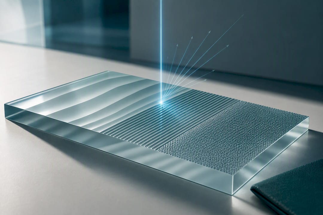
Different instruments see different slices of the same surface, and that is the single biggest source of disputed acceptance reports. Atomic force microscopy (AFM) offers the finest vertical and lateral resolution, resolving true nanoscale roughness, but its scan area is typically limited to tens of microns, so it can miss mid-spatial structure entirely. Stylus profilometers cover larger areas and are robust for production floors, but the physical tip radius limits lateral resolution and can flatten sharp features. White-light interferometers and non-contact optical profilers scan faster over wider fields and suit production QA, though their vertical sensitivity depends heavily on the surface’s reflectivity and slope.
Comparative testing on glass-ceramic substrates has shown that AFM, stylus and optical profiler measurements of the same surface diverge06764-7) depending on scan size and sampling interval, so a single instrument’s number is rarely the whole story.
- Match the instrument to the spatial band you care about — AFM for true roughness, interferometry or PSD-capable optical profilers for mid-spatial error.
- State the filter and sampling length on every acceptance report, not just the resulting Ra or Rq.
- Request multiple scan locations, since a single point measurement on a large aperture tells you almost nothing about uniformity.
- Reference ISO 10110-8 on the drawing, which defines how surface texture and defects should be specified and reported for optical elements.
Pro Tip: Ask any supplier for the PSD plot alongside the summary Ra/Rq figures. If they can only provide one number with no bandwidth stated, treat the report as incomplete, not final.
Precision Glasses’ own measurement methods guide walks through instrument selection in more depth for teams writing their own test plans.
What roughness actually costs you: scatter, haze and coating failures
Roughness translates into optical loss through the bidirectional reflectance distribution function (BRDF), which describes how light scatters away from the ideal reflected or transmitted direction. Fine-scale roughness scatters light at wide angles, producing haze; mid-spatial roughness scatters closer to the specular direction, degrading contrast and beam quality without necessarily showing up as visible haze at all.
Application thresholds vary sharply by use case. High-precision imaging and laser optics generally need sub-nanometre Rq and tightly bounded PSD. Consumer and industrial displays tolerate more, and anti-glare surfaces are deliberately roughened, trading some clarity for reduced glare; haze in that range typically sits between 1% and 8% for high-precision displays, up to 45% for outdoor readability where sparkle and glare matter more than pixel-level sharpness.
- Excess roughness scatters laser light and can lower damage thresholds in high-fluence applications
- Coating adhesion sometimes benefits from controlled micro-texture, which increases surface area for bonding
- Uncontrolled roughness under a coating instead traps stress and promotes delamination
- Densification during polishing can raise scattering even when RMS roughness itself is very low, an effect confirmed in studies of polished fused silica
Reducing roughness: polishing, laser smoothing and coatings compared
Chemical-mechanical polishing (CMP) remains the workhorse process for optical glass, and its outcome depends far more on slurry particle size distribution, pad topography and slurry chemistry than most specifications acknowledge. Predictive models such as the Ensemble Hertzian Multi-Gap and Island Distribution Gap frameworks link these polishing variables directly to both removal rate and resulting microroughness, giving engineers a way to reason about process windows rather than treat polishing as a black box.
- CMP with controlled slurry PSD and pad selection achieves the lowest roughness figures available; recent work with dual-size nano CeO2 slurries reached the sub-angstrom range on fused silica, an extreme end of what production processes can target.
- Balancing mechanical and chemical polishing action is the primary lever for suppressing mid-spatial-frequency error, since excessive chemical action during polishing is a known source of MSFE.
- Laser smoothing and chemical etching can reduce sub-micron roughness on some glass types without full re-polishing, useful for localised repair, though they carry their own risk of introducing new form error if not tightly controlled.
- Wet blasting and anti-reflective or anti-glare coatings trade optical clarity for durability or glare control; AG coatings intentionally add controlled haze, and above roughly 30% haze the relevant test standards shift from clarity-based metrics to total transmission measures.
Pro Tip: Never accept a “polished to specification” statement without a test report. Ask what slurry PSD, pad type and number of measurement scans were used, since those three variables determine whether the result is repeatable across a production batch.
Fabrication contamination during finishing also degrades apparent surface quality regardless of the polishing recipe; the surface protection guidance from Dust Free Film on defect control during finishing stages is a useful cross-industry reference for keeping particulate contamination out of a clean-room polishing environment.
How Precision Glasses manages surface quality from design to delivery
Precision Glasses builds roughness control into every stage of the fabrication lifecycle rather than treating it as a final inspection step. Design review sets the target metric and sampling length before material selection begins; machining and polishing stages apply controlled slurry and pad parameters matched to the substrate; coating and final inspection close the loop with traceable quality assurance documentation. When requesting a quote, specify the metric (Ra, Rq or PSD), sampling length, required instrument, and the number of measurement locations you expect on the test report. That level of specificity is what separates an audit-ready acceptance document from a single vague number on a certificate. Details on the precision glass manufacturing workflow outline how each checkpoint fits together.
An engineer’s checklist for reviewing supplier quotes
Before signing off a quote, confirm the drawing states the metric, sampling length, instrument and any PSD requirement. Ask the supplier how they verify process repeatability across a batch, not just on a single sample. Treat vague specs, unstated bandwidths or single-point measurements as red flags worth pushing back on before the purchase order is issued.

Get roughness right the first time with Precision Glasses
Generic polishing shops quote a single Ra number and hope it holds across a production run. Some precision manufacturers build the acceptance criteria into the process before the first part is cut, so the test report matches what the drawing actually asked for.

The company’s services span glass cutting, CNC machining, edge finishing, toughened and laminated glass, and AR/AG coatings, while the optical components line covers achromatic lenses, aspheric lenses, cylinder lenses, beam splitters and optical filters manufactured to tight figure and roughness tolerances. Every order carries traceable, ISO 9001-certified quality control, with inspection data documented from prototype through to volume production. If your drawing needs a defined Ra, Rq or PSD callout and a supplier who will actually report against it, submit your drawing through the services page and request a measurement plan alongside your quote.
Standards and research worth reading next
- ISO 10110-8 for surface texture specification on optical drawings
- Fused silica super-polishing with dual-size nano CeO2 for state-of-the-art achievable roughness
- Densification and scattering in polished fused silica for why low Rq does not always mean low scatter
- Roughness scaling at the nanoscale for how measurement resolution changes what “roughness” means
Sources
- Fused silica with atomic-level super-smooth surface manufactured by dual-size synergistic nano CeO2 and its highly efficient polishing mechanism
- The densification characteristics of polished fused silica glass and its scattering characteristics
- Roughness and scaling properties of oxide glass surfaces at the nanoscale
FAQ
What is 0.8 Ra surface finish?
A moderate finish used on many mechanical glass and metal surfaces has average roughness deviations far above those for precision optics. Optical-grade windows and lenses usually require values in the nanometre range, measured with a defined sampling length as covered above.
What is the 16% rule for surface roughness?
There is no single universal “16 rule” recognised across optics and machining standards, and definitions vary by industry context. In some manufacturing conventions it refers to a statistical acceptance approach where no more than roughly 16% of measured peaks may exceed a stated roughness limit, but engineers should confirm the specific convention their drawing or standard references rather than assume one universal figure.
How do I calculate surface roughness?
Ra is calculated as the arithmetic mean of the absolute height deviations from the mean line across a defined sampling length, while Rq (RMS) squares each deviation before averaging and taking the square root, weighting larger defects more heavily. Both require a stated sampling length and filter cutoff to be meaningful, and instruments like profilometers and optical profilers can report different values for the same surface depending on scan parameters.
What does 3.2 surface roughness mean?
A callout of this kind typically refers to a relatively coarse finish suited to structural or non-optical glass surfaces rather than precision components. For optical windows, sensor covers or lenses supplied through Precision Glasses’ optical components line, target figures are usually specified in nanometres, reflecting the far tighter scatter and haze requirements of those applications.
Why does my part pass Ra but still scatter light badly?
A single Ra value averages out spatial structure and can hide mid-spatial-frequency error that scatters light without raising the overall roughness number. Requesting a PSD plot alongside Ra and Rq, as outlined in the metrology section above, is the reliable way to catch this before the part reaches final assembly.